Date: Sat Sep 8 13:10:34 2001
Posted By: Eric Maass, Director, semiconductors / communication products
Area of science: Computer Science
ID: 999900588.Cs
Message:
Hi Brittany. I'm guessing, but I think maybe your assignment was to interview a scientist and find out what basic question that scientist had tried to answer, and whether that scientist was
successful in answering the question. I'm guessing this because -- well, there is no ONE question that all scientists are trying to answer. There are many fields of science, each with their
own puzzles and questions that scientists try to answer and understand better.
So, I will try to answer with one example from my own career. When I was in research back in the 1970's, we were trying to make very small MOS (Metal Oxide Semiconductor)
transistors. Here is a sketch of an MOS transistor:
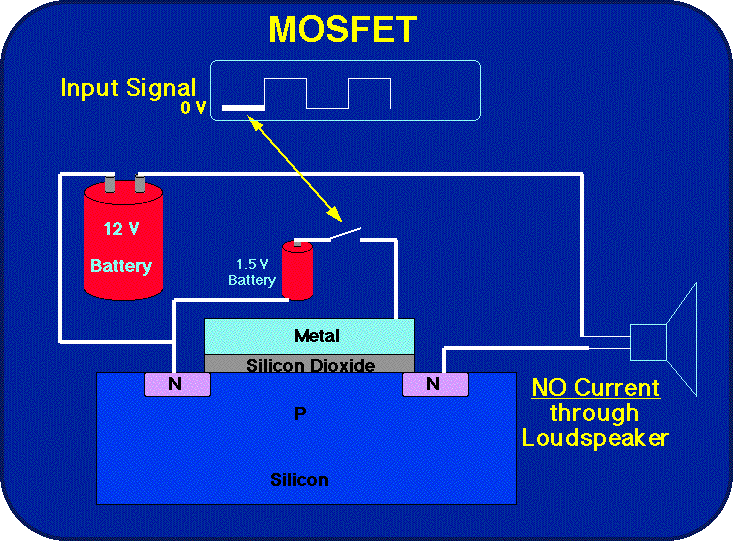 Notice the area labeld "Silicon Dioxide" under the metal. Silicon dioxide is basically the chemical that glass is made of. Silicon dioxide, like glass, is an insulator - it doesn't conduct
electricity.
In order to make smaller transistors, one of the questions we had to answer was whether we could make that layer of silicon dioxide much thinner, and still have it act as an insulator. While
we had been making MOS transistors with a silicon dioxide layer that was about .1 micron (.1 millionth of a meter, or a ten thousandth of a millimiter) thick, but for the smaller transistors ,
we had to make the silicon dioxide layer only .02 microns thick - a fifth as thick! The layer was made up of lots of silicon and oxide atoms -- and at .02 microns, we are talking about a
layer only a few tens of atoms thick. There were people who said that that thin of a layer would not act as an insulator...there were all sorts of hypotheses that the electrons that carry
electricity would pass right through the silicon dioxide if it was only .02 microns thick.
So, I decided to try to answer that question by making MOS transistors with that thin of an oxide. I also wanted to answer some other questions about making the tranistors smaller side to
side - the spacing between the two regions labelled as "N" in the image above is called the "gate length". At that time, the transistors had a gate length of about 3 to 5 microns (3 to 5
thousandths of a millimieter). So, I came up with a way to try to make MOS transistors with a 1 micron gate length and a .02 micron thick gate oxide.
I did a lot of research, and developed a process that I thought had the best chance of making a good quality oxide and make the gate length small without causing the two N regions to get
so close that they would touch in any way. Then, I ran the experiment with the help of a lot of good people.
When we finished the experiment, I measured the gate length using an electron microsope. The gate length was right at 1 micron - so far so good. I used a technique called CV plotting to
look at the capacitance of the silicon dioxide, which helps you determine the thickness..it was right at .02 microns...right on target.
Then it was time for the key question - would the transistor work, or would it leak too much? So, I hooked up electrodes to the transistor, and measured all the currents with different
voltages applied...yes, it worked, and there was almost no leakage!!
At the time, this was the smallest transistor successfully made in the world.
Nowadays, we routinely make much smaller transistors than I made then...but at the time, it answered a question that many scientists and engineers were concerned about.
I hope that gives you an idea for your assignment. Have a great weekend!
Notice the area labeld "Silicon Dioxide" under the metal. Silicon dioxide is basically the chemical that glass is made of. Silicon dioxide, like glass, is an insulator - it doesn't conduct
electricity.
In order to make smaller transistors, one of the questions we had to answer was whether we could make that layer of silicon dioxide much thinner, and still have it act as an insulator. While
we had been making MOS transistors with a silicon dioxide layer that was about .1 micron (.1 millionth of a meter, or a ten thousandth of a millimiter) thick, but for the smaller transistors ,
we had to make the silicon dioxide layer only .02 microns thick - a fifth as thick! The layer was made up of lots of silicon and oxide atoms -- and at .02 microns, we are talking about a
layer only a few tens of atoms thick. There were people who said that that thin of a layer would not act as an insulator...there were all sorts of hypotheses that the electrons that carry
electricity would pass right through the silicon dioxide if it was only .02 microns thick.
So, I decided to try to answer that question by making MOS transistors with that thin of an oxide. I also wanted to answer some other questions about making the tranistors smaller side to
side - the spacing between the two regions labelled as "N" in the image above is called the "gate length". At that time, the transistors had a gate length of about 3 to 5 microns (3 to 5
thousandths of a millimieter). So, I came up with a way to try to make MOS transistors with a 1 micron gate length and a .02 micron thick gate oxide.
I did a lot of research, and developed a process that I thought had the best chance of making a good quality oxide and make the gate length small without causing the two N regions to get
so close that they would touch in any way. Then, I ran the experiment with the help of a lot of good people.
When we finished the experiment, I measured the gate length using an electron microsope. The gate length was right at 1 micron - so far so good. I used a technique called CV plotting to
look at the capacitance of the silicon dioxide, which helps you determine the thickness..it was right at .02 microns...right on target.
Then it was time for the key question - would the transistor work, or would it leak too much? So, I hooked up electrodes to the transistor, and measured all the currents with different
voltages applied...yes, it worked, and there was almost no leakage!!
At the time, this was the smallest transistor successfully made in the world.
Nowadays, we routinely make much smaller transistors than I made then...but at the time, it answered a question that many scientists and engineers were concerned about.
I hope that gives you an idea for your assignment. Have a great weekend!
Current Queue |
Current Queue for Computer Science |
Computer Science archives
Try the links in the MadSci Library for more information on Computer Science.
MadSci Home | Information |
Search |
Random Knowledge Generator |
MadSci Archives |
Mad Library | MAD Labs |
MAD FAQs |
Ask a ? |
Join Us! |
Help Support MadSci
MadSci Network,
webadmin@www.madsci.org
© 1995-2001. All rights reserved.