| MadSci Network: Physics |
When we start to talk about electrons and holes with relation to semiconductors and circuits, it can get pretty confusing. My background is in chemistry and engineering, so the way that I try to understand these issues may be different from that of an electrical engineer or a physicist, so if I have some of the details wrong, or if your understanding is different, then please feel free to correct me; I won't be offended.
Now, let's first start talking about semiconductors, the materials used to make diodes, transistors, and just about everything associated with electronics today. There are two types of semiconductors, those that contain an excess of electrons (referred to as "N" type semiconductors) and those that have spare places for electrons to park, which are referred to as "holes." These types of semiconductors are referred to as "P" type semiconductors. Whether a semiconductor is an N type or P type semiconductors depends on the type and amount of chemical impurity contained within the semiconductor. Without these impurities, the semiconductors would be essentially non-conductors.
In the same bar of semiconductor, you can have one region of the semiconductor with the N type impurity, and another part of the semiconductor with the P type impurity. Where the two types of impurity meet is where all the magic happens. I drew a little drawing to illustrate my understanding of what happens at this junction.
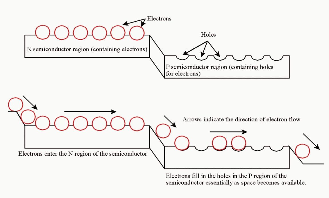
In the upper left portion of this picture, there is an N semiconductor region, containing a bunch of electrons. I have colored the electrons red to make them so you can distinguish them from the semiconductor, and because I like to think of electrons as hot, i.e. they are ready to do some work. If these electrons look like marbles, rolling down a ramp, then, that's OK; its hard to imagine what a real electron looks like as it passes through a wire because they are so small. In the upper right portion of this picture there are "holes" or spaces where the electrons can sit (even if only for a moment). Now, in this particular semiconductor, the electrons in the N region are resting comfortably, but if you give them a bit of a push, they will all shift to the right, with the electron on the right able to run down the hill and fill one of the holes waiting for it. Once on the bottom side of the hill, the electrons can again shift toward the right, making another space or hole for the next electron in line to fill.
So in the bottom portion of this drawing, you can see new electrons entering down the hill on the left, traveling across the N material, running down a steep hill to fill spaces as the open up in the P material. The electrons in the P portion of the material keep shifting right until they exit the semiconductor. Now, here is the confusing part; every time an electron moves right in the P material, it opens up a spot or hole on its left, so in a sense, the holes are moving to the left while the electrons are moving to the right.
There are two other things to notice in this drawing. As the electrons travel down the hill between the N region and the P region, they pick up speed (that's why it is a hill). To slow down and settle into a hole, if even for a moment, they have to give up this energy. The energy can be emitted by heating up the surrounding material, or it can be emitted as infrared, visible, or UV light. In what form the excess energy is given off in is a function of the type of semiconductor material.
The second thing to notice is that if we tried to bring in a bunch of electrons from the right, we would initially fill up all of the "holes" and we could try and get the electrons to run uphill into the N region, but once there, there is really no place for a new electron to squeeze in. And that is how it works in diodes; electrons can travel in one direction, but they really have a difficult time traveling in the opposite direction. You can try to force the electrons to move in the reverse direction by applying a lot of force (voltage) but it will get everyone hot, and will tend to burn up the semiconductor. So, as long as you operate a diode within certain voltage and current limits, it will work very well at allowing electrons to move in one direction through it, but will block electrons from traveling the other direction.
Now, we get to the issue of what is happening in the rest of the circuit. As you may notice, there is really nothing in the diode structure that limits how rapidly the electrons can pass through. If we had a large supply of electrons, then you can imagine that a large number might flow through the diode at the same time. If too many try and pass through the diode at the same time (while each one gives up the same amount of energy) then the diode will overheat and burn up.
I have another drawing to try and help answer the second part of your question.
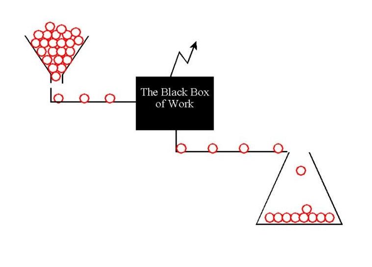
In the left of this image, a bunch of electrons are stored in a container. This particular container has a funnel shape so it restricts the flow of electrons (imagine that we are using a watch battery instead of a car battery that can supply a huge amount of electrons). The electrons flow out the base of the container, and travel into the "Black Box of Work." In our discussion, this black box of work could be a light emitting diode, a light bulb, an electric motor, a heater or any other device we might try and power.
The electrons enter the black box, they perform whatever magic is needed within the box (perhaps involving P and N junctions, holes, electrons, quanta of emitted energy, etc.), and then they drop out of bottom of the box. As they enter the box, they are rather energetic; as they exit the box, they have lost most of their energy and are just looking for a quiet place to rest. In some cases, if you don't work the electrons too heavily, you can put a couple of Black Boxes of Work in a series, powering each of them in turn with the same electrons. One black box might produce light every time electron enters into it. A second black box might contain an internal switch that might turn the flow of electrons on and off automatically several times a second. It really doesn't matter what each particular box does so long as we don't try and get them to do something they can't do.
The as the electrons exit the black box of work, they run into a container at the bottom right of the picture; let's call it the used electron container. Now, throughout this description, the electrons are in a line, waiting their turn. If we run out of electrons in the funnel shaped container supplying electrons, then everything will stop. If the used electron container gets completely full, then again, the movement of electrons stops and no further work is done.
If the device powering this circuit is a battery, you might imagine that one end of the battery is the source of supply of new, energetic electrons, while the other end of the battery is the used battery container. So electrons flow out one end of the battery as they return into the other end.
Now, I know my description is not complete; we haven't discussed why the energetic electrons want to exit one end of the battery, and are willing to enter into the used electron container portion of the battery. But hopefully the information I have provided might give you a bit more insight into what is going on within a diode, as well as an electric circuit generally.
Try the links in the MadSci Library for more information on Physics.